


Bigger, better, faster: Introducing the Nix Badge 2.0
Four days in Vegas. Two NixOS installs. One SD card.
by Morgan Jones and the Nix Vegas #badgelife team
We decided to do a very hard thing for Hacker Summer Camp this year. At the height of component shortages, we built a whole single board computer and shipped it by DEF CON.
It was bigger than last year's badge by about an inch on the diagonal. It was better, with ethernet, HDMI, real SDIO, real USB, and a dedicated debugging bridge. And it was faster, running parallel NixOS installs on either an ARM or RISC-V core from the same SD card. Yep, it booted Linux.
We're very proud of this labor of love for the Nix community, and were excited to share it with our speakers at Nix Vegas, and now you.
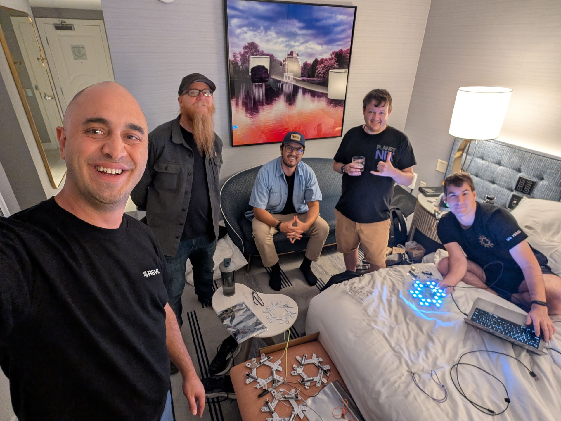
The Nix Vegas #badgelife team
Links
We have heard very strong feedback that people want these. We have some v2.0 hardware badges left, but need to figure out how to sequence another run (v2.1, likely with some hardware tweaks). We'll see about launching on CrowdSupply soon as they closely fit our values as an open source project; stay tuned.
This blogpost has a companion talk at NixCon this year, maybe we'll have more information by then.
If you think this is cool and want to sponsor us, reach out at sponsor@nix.vegas or see our sponsorship prospectus.
defcon: 33 -> 34
Our badge at DEF CON 33 was based on the ESP32-C6. It had 12 LEDs, and ran on 3xAAA batteries. Since it was our first time making a DEF CON badge and all of our first year running the Nix Community, we decided to keep it relatively simple. Of course, we added a bunch of features to it too, and implemented the Nix store's HTTP binary cache protocol as a bonus.
We wanted more for DEF CON 34, though. We still loved the idea of badges running a binary cache, but quad SPI to the SD card on the ESP32-C6 was not a recipe for anything resembling speed. We even tried it. With an interposer to fix our broken SD pinout, serving NARs over wifi was extremely slow. Not exactly sustainable for a cache.
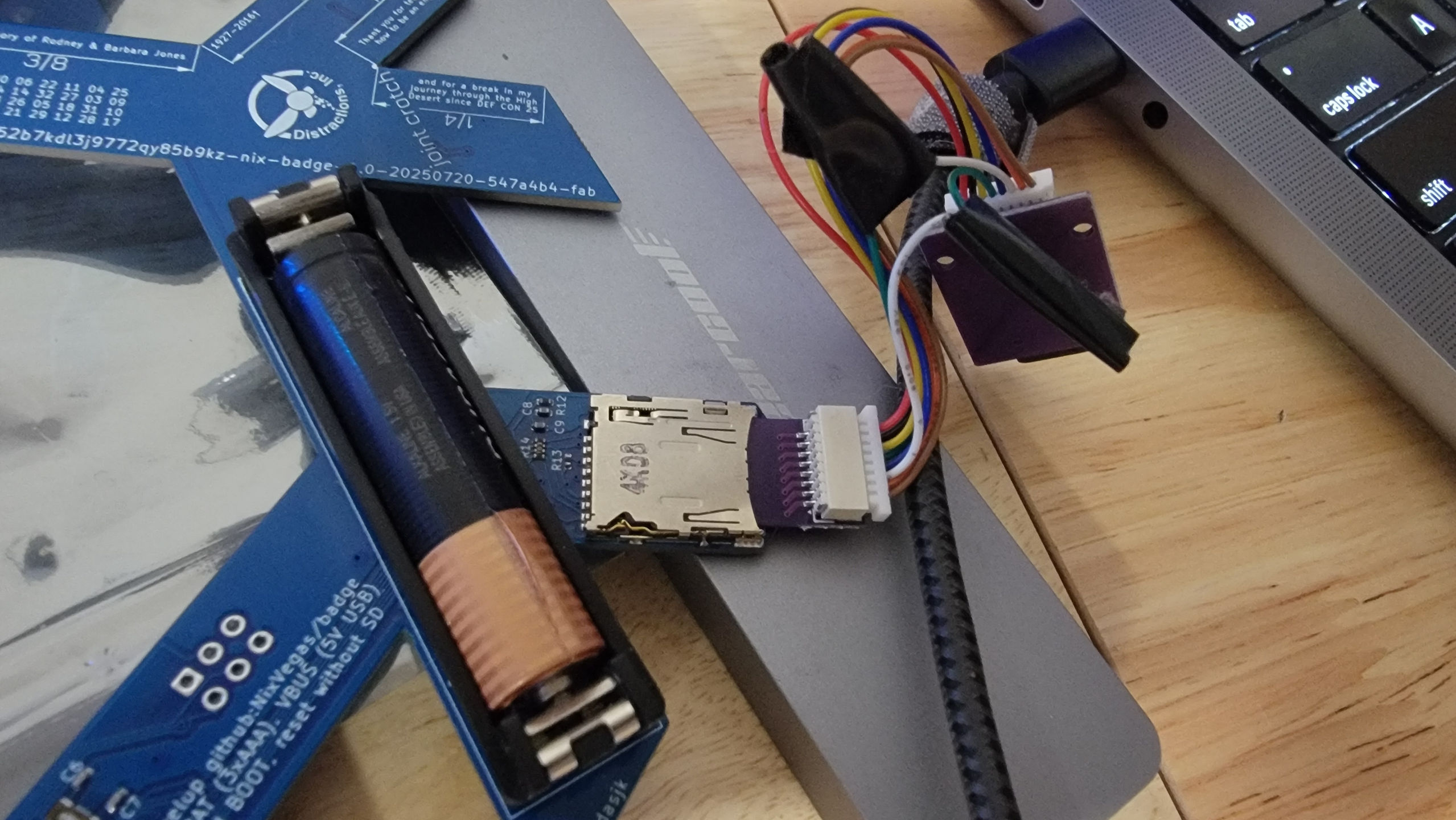
Modern problems, modern solutions, etc.
And, since we accidentally ordered a ton of AA batteries for our badge last year due to an Amazon misclick, the badge this year needed to use them somehow.
Playing SoM Roulette
We experimented with a few options. A system-on-module was probably easier to get working for a badge than a system-on-chip and discrete DRAM, so we leaned that direction first. On the SoM side, we picked up a dev board for the Milk-V Duo Module 01 and looked at the Waveshare ESP32 P4 because it also had high-speed SDIO and ethernet. On the SoC side, we managed to get our hands on what was likely the last OrangeCrab available so we could play with a Lattice ECP5.
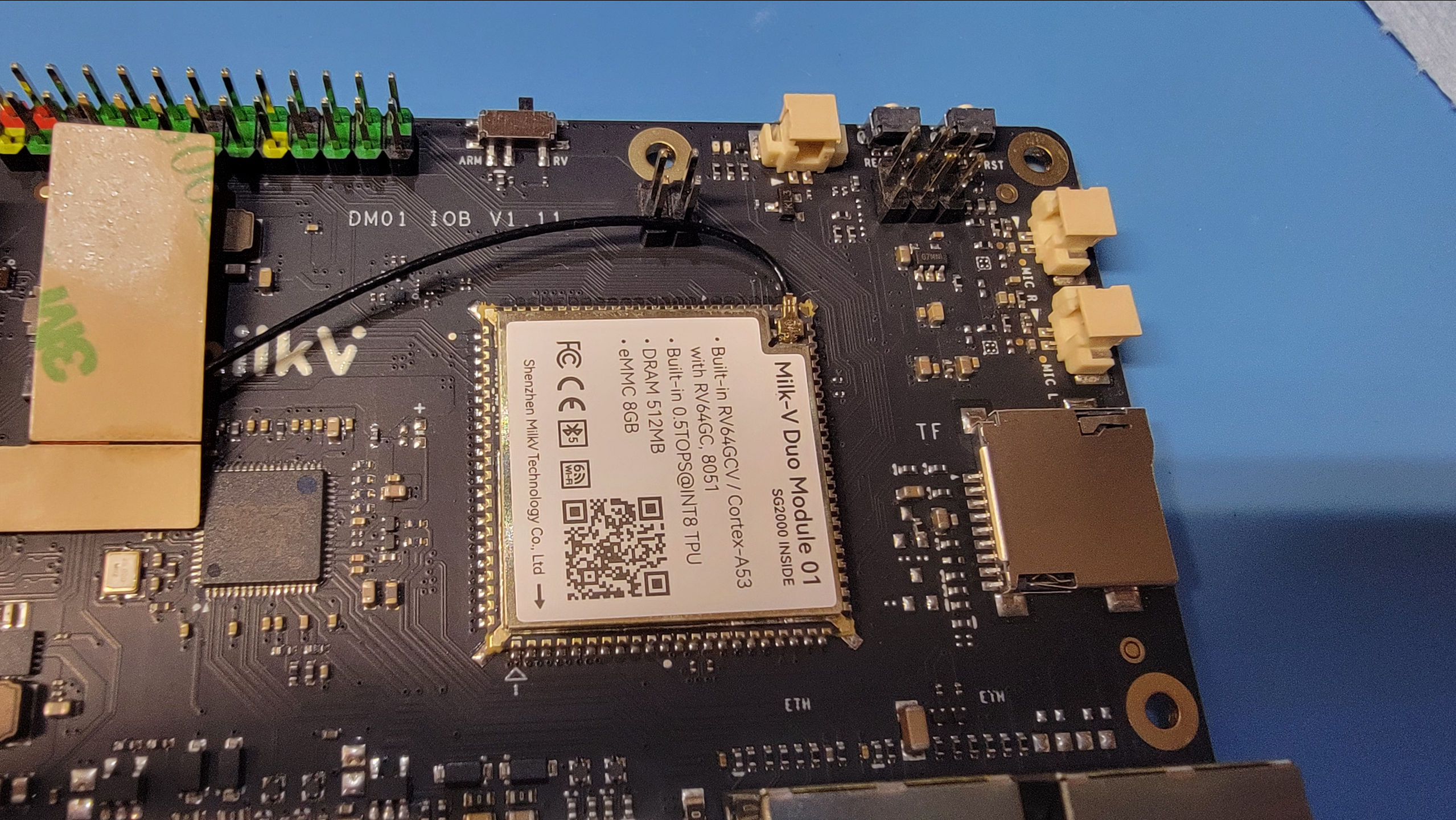
A Milk-V Duo Module 01 dev board, ready for action
While the ECP5 is a formidable chip (and the Cam Link 4K we used to run our stream and talk recordings is actually based on one), Lattice does not include a hardware DRAM controller, so you are stuck implementing DRAM training and signaling yourself in Verilog or your wrapper of choice. You also have to route some flavor of DDR, which is expensive, time-consuming, and error-prone (though newer tooling is making it less so). It would also add more layers to the badge unless we did a small daughterboard (effectively, making our own SoM). These strongly looked like "next year" items for us.
We ultimately decided to go with the Milk-V Duo Module 01 despite the supply chain being a potential issue. We knew it worked, we knew it could boot NixOS from experimenting with it, and the Waveshare P4 happened to have roughly the same 88-pin footprint within a couple millimeters (either convergent evolution, or one company copied the other).
Given the choice between spending a ton of time routing a SoM that could boot NixOS on a badge and one that couldn't, the choice was clear. The theme of DEF CON this year was Agency, and we had to just go for it. The only thing that's more "agency" than dual booting ARM and RISC-V would be putting a full FPGA on the badge or doing custom silicon like Bunnie did, and we didn't want to bite that off this year.
Reproduce This Build
We had our reproducible build pipeline and KiCad project from last year, so started there. We were sponsored by PCBWay rather than using JLCPCB this year, so had to make a few very minor changes to the output format. The two fab shops use the exact same Gerber format, so Fabrication Toolkit worked just fine as it did last year.
PCBWay also allows slightly tighter routing tolerances, so after a few DRC modifications, things mostly just worked. After breaking our build process into multiple derivations, we recompressed our Gerber output using 7zip solid mode, since PCBWay has a 100 MiB file limit but accepts 7zip, and this allowed us to meet it.
AI is actually useful
Restoring sanity to PCB design and embedded development is one of the most important things I've seen AI tools be able to do. If you're reading this and thinking "oh no, this badge is going to be a bunch of slop..." no, it was mostly designed by hand. But... some of the most convincing arguments I've seen for why it's useful have to do with component datasheets and reverse engineering hardware.
Using a skill to fuzzy search LCSC, download and translate datasheets, and spit out KiCad components and schematics with easyeda2kicad (also in nixpkgs) was amazing, full stop. At the very least, it allowed me to do things like ask what buck-boost converters were common, what their supply was on LCSC, and then do things like converting that into an approximate schematic that I could then manually refine, place, and route, along with a first pass at device tree nodes. It also helped search, translate, and interpret 300 page CPU datasheets when I do not speak Chinese. Simply put, the LLM can fill in the gaps you have in your knowledge if you work with it.
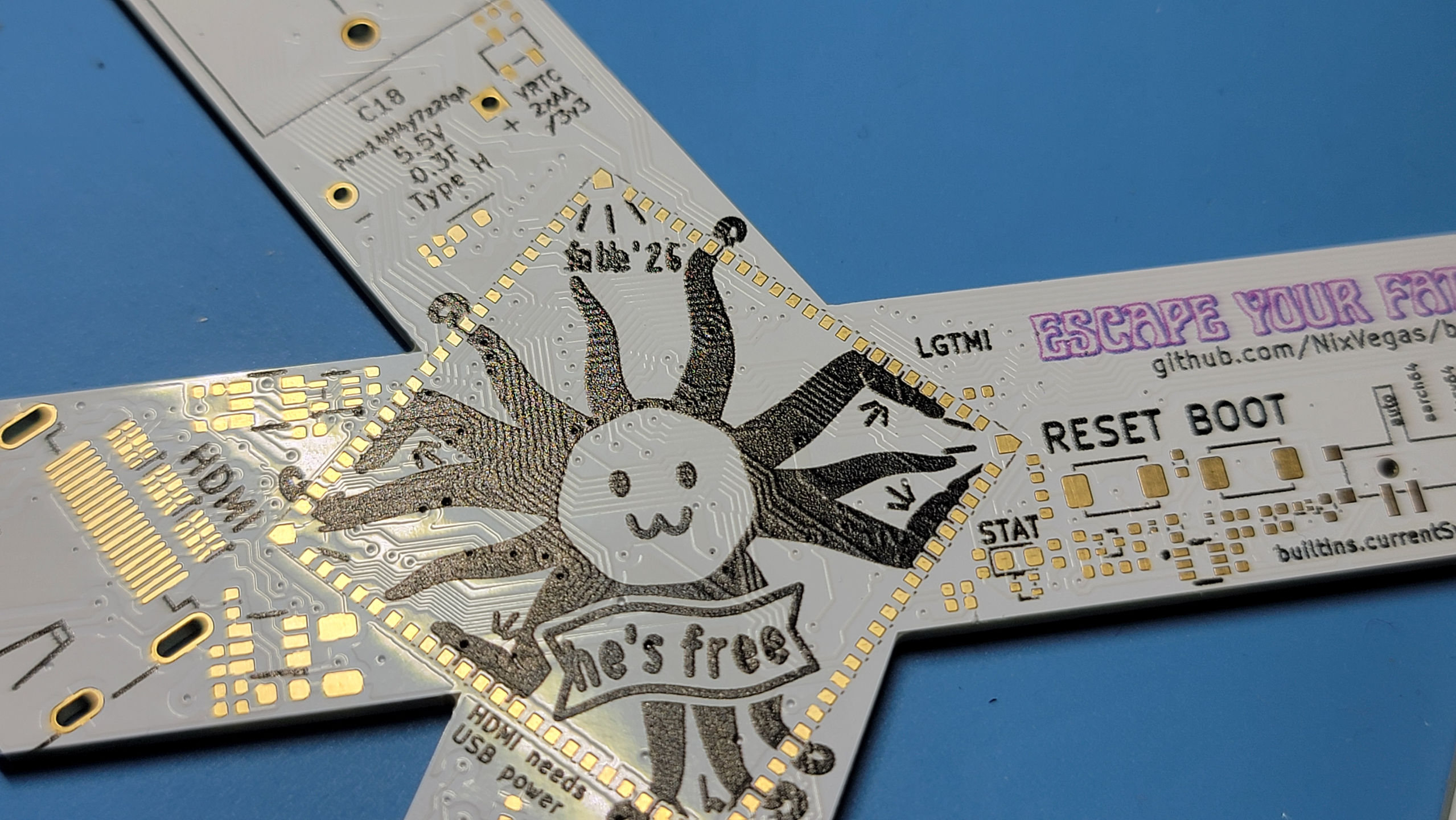
Fable did a self portrait as an octopus escaping a jar (but it was our SoM, and we got mask ROMs)
Frontier models that can preflight check PCBs for errors are massively underrated. Fable found multiple subtle mistakes, including a couple major schematic issues (the data lines on our SD card were swapped around, for example). This is the exact kind of thing that's really error prone if you're doing it by hand, but a robot that can use KiCad's Python API to dump netlists will identify the error quite quickly.
Parts substitution is also exactly the thing a LLM is good at. PCBWay gives you an Excel file full of your components and whether they have them, and the estimated lead time. Throwing it at Fable and a LCSC search tool will immediately help to repopulate it with confirmations, corrections, or redirections. It can then apply these back to your repo so you simply do not have to do so by hand.
And, nixpkgs offers 140K+ tools, which is perfect for an agent driving long processes.
Embedded development is fun again
Researching upstream trees of various Debian sources was also quite useful. If you use the LLM as a research assistant alongside normal grep, you can identify how certain configs and modules are defined in context of kernel sources and strange Debian-style polyrepo setups, which informs what you may be missing when porting NixOS. You can kick these processes off, go do something else, and come back with a report (in somewhat tortured English) of the load-bearing things that it found. While some things may be hallucinated, you can go and prove or disprove those claims on your own, but you at least have a starting point.
The iteration process with hardware is often trial and error anyway, with unreliable documentation and legacy code everywhere. Sometimes, knowing what doesn't work is just as informative, and trying it fast is the difference between having a badge at DEF CON and not having one.
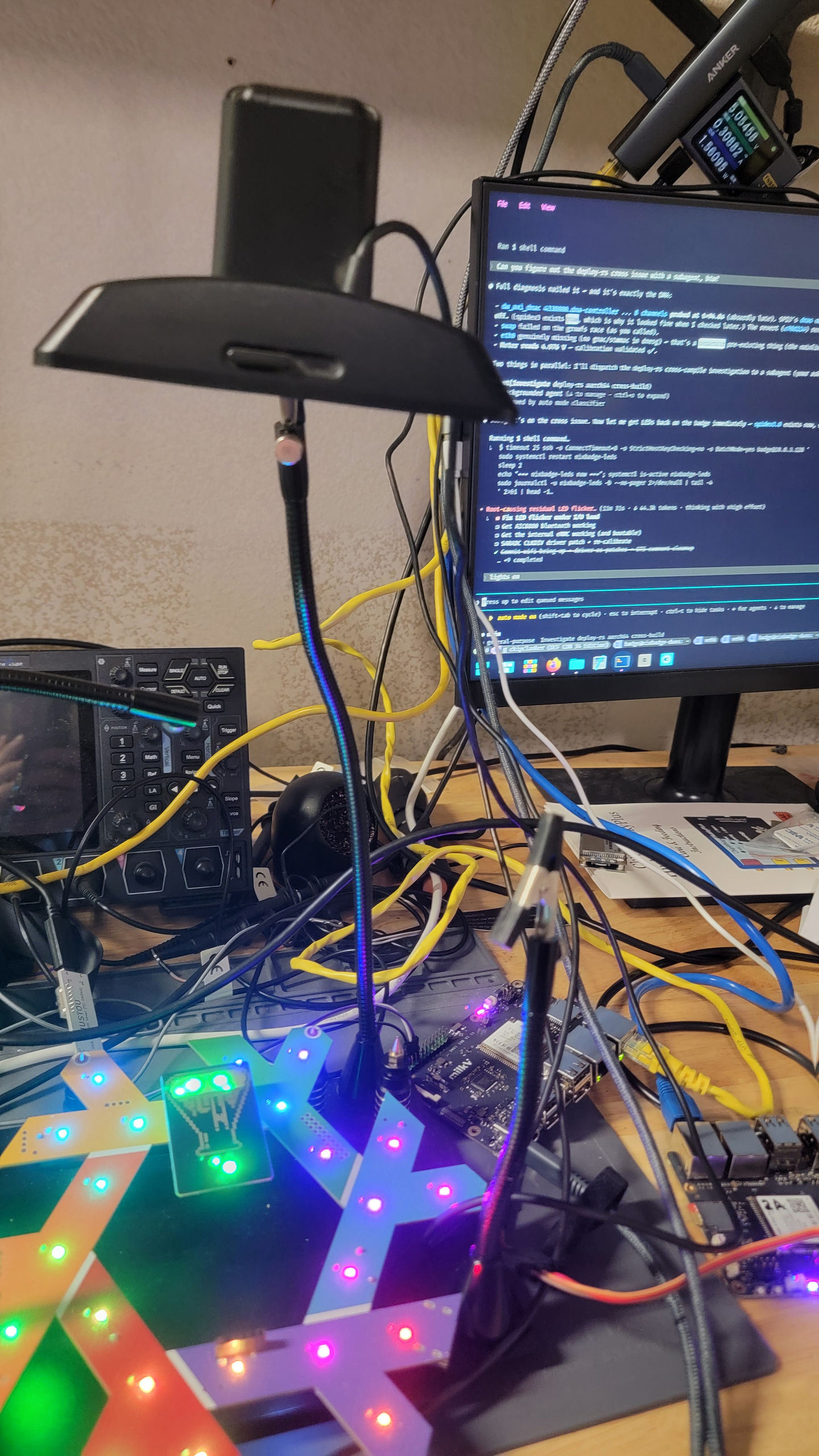
Automatic iteration on hardware bringup FTW
These are all processes that are ordinarily more time-consuming than they could
be, and the best usecases for AI! When all you have are PDFs and a LLM that can
wield nix run nixpkgs#poppler-utils and knows other languages better than
you, it is likely wise to offload things that are effectively hard labor to it
so you can focus on the things it cannot do. For me, this was routing,
silkscreen, and the features of the badge itself. Search, error checking, and
some aspects of component selection were squarely in the LLM's wheelhouse, as
was helping to try things with the hardware.
The agent's box was a Protectli VP2420 connected over our 802.11s mesh network to our huge remote builder. It had access to a ChipWhisperer Husky (where I managed to help it automate power analysis and fault injection against the example target boards and could recover a RSA key from a Lattice iCE40 FPGA in 2 minutes, but that's another blogpost).
Making a SBC
With all the annoying things suddenly easier, it was time to design an SBC and not have it feel like work. We added all the trimmings for maximum hackability: LEDs, connectors for SAO and small OLEDs, USB, ethernet (the Sophgo SG2000 has a built in 10/100 ethernet PHY whereas the Waveshare module certainly does not), a CH347 serial/JTAG to USB adapter, USB mode switching circuitry, a supercap for keeping the RTC alive between battery swaps, and even a DSI to HDMI adapter.
The boot selection switch was particularly interesting. Since the ARM and RISC-V cores are strapped with a hardware pin from the mask ROM, I settled on a three way switch, with "auto" wired to a latch on the always-on RTC bus. Linux can control it with a GPIO, or you can manually override it to the ARM or RISC-V core. At the end of the day, the ARM core was the faster one (the RISC-V core was an Alibaba one), so we manually moved the switch there for everyone.
Regardless, our testing showed that the mask ROM looks for a fip.bin in the
first FAT32 partition for the correct architecture, so switching between ARM
and RISC-V requires a minor SD card change too. We'd certainly like this not
to be the case, but it will take a bit more research, although we may have
figured it out while writing this blogpost. (In the meantime, we created a
nix-badge bootswap command to do exactly this).
KiCad 10 routing woes
Component selection and placement was done, it was time for routing.
KiCad had some major stability issues this year for us since the recent 10.0 update. It seems like it was mostly happening on an older Haswell and a newer Ryzen 5 Framework laptop that was being frequency throttled. I bet that the situation improves over time, but we had enough on our PCB that KiCad was constantly unstable when working with it, even after I merged an update.
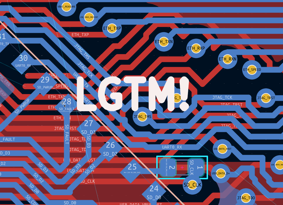
Didn't stop all the crashing, but shipped on the badge.
However, a good Nix environment and enough in-repo scripting was enough to puppet KiCad's Python API and make targeted board changes when the UI failed us. There's also tscircuit and atopile now, maybe we'll use these next year too.
Still, we couldn't fully escape placement and routing. The initial routing pass for the Nix Badge v2 was ~10 days of solid work in the evenings and weekends. I am hoping the tools improve, but am skeptical about how much. There is a lot of project context that automatic placement will simply not always get right. PnR is also usually tuned to contiguous geometric shapes, and the Nix logo, while mathematically perfect, is not pleasing for an autorouter due to the gigantic hole in the middle. For the "I want to do one targeted change" usecase, automation worked fine.
Colored silkscreen
Our badge had our art and the NixOS pride colors on it. For our first test of PCBWay's colored silkscreen service, it passed flawlessly.
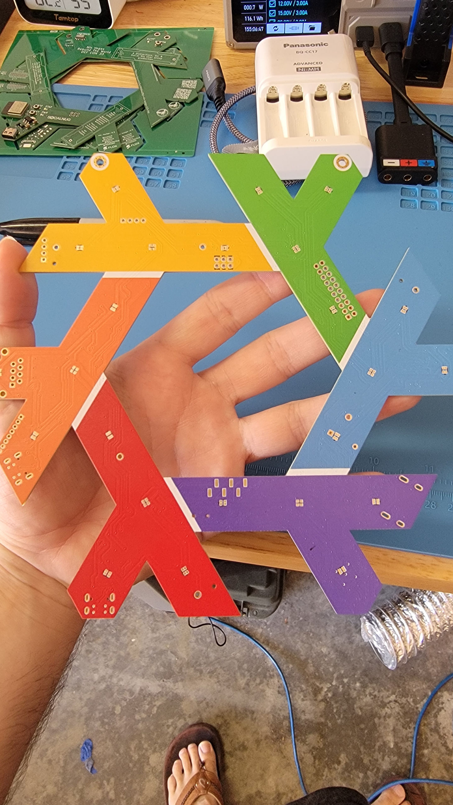
Samples from PCBWay arrived and they looked amazing
In any case, I haven't found many people writing about how to actually use PCBWay's UV printing, so feel like I need to go into detail here, since having this information would have saved us multiple design iterations (which is a typical thing that people ignore when pushing the red button on a PR they don't like, but I digress).
There is no standard way to do colored silkscreen in PCB design, period. There simply aren't standard Gerber layers for it, and KiCad 10 does not support anything beyond monochrome silkscreens with overlaid reference images. In fact, if you import a colored SVG such as a vectorized version of our art, KiCad will convert it to a monochrome point cloud, throwing out any bitmap data and all of the information about colors, vector layers, and even rotation.
We ended up writing scripts (with a little help from Fable 5) that could recover SVG layout from KiCad's point clouds with a little linear algebra, and compile master SVGs from the originals in the repo with position, scale, and rotation implicitly indicated in the KiCad project. This allowed us to use KiCad mostly as normal, and pushed the color silkscreen generation (including merging text layers and solder mask knockouts) to be part of the build process. It also would let us gracefully degrade to monochrome silkscreen for PCB fabs that don't support color as part of their process.
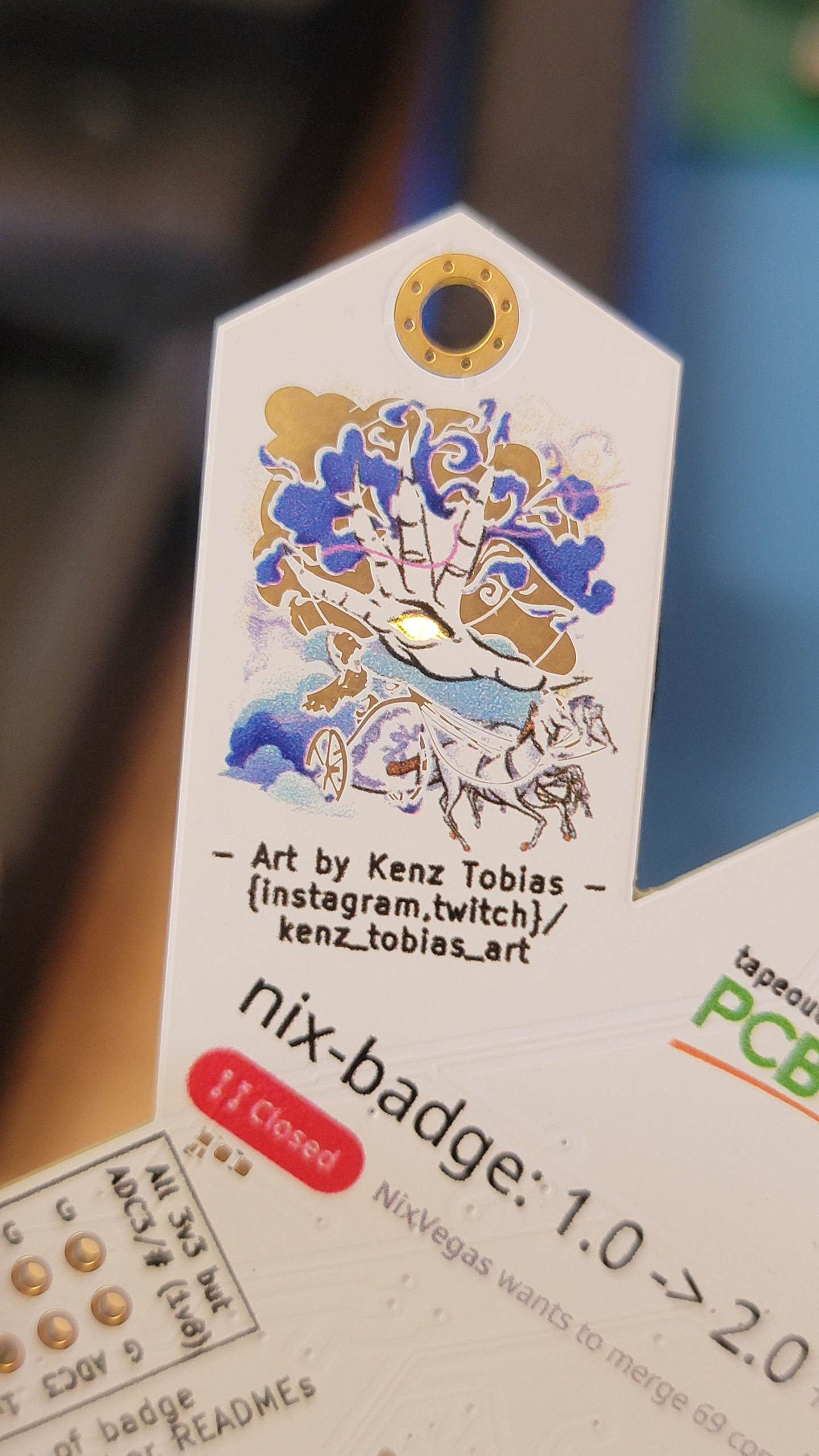
Solder mask knockout behind the eye with rear illumination. We'll knock more out on v2.1 so the LED shines through better.
PCBWay (as opposed to JLCPCB) does not require a strange encrypted SVG format for their colored silkscreen. Instead of vendor locking you to EasyEDA, you simply provide high-resolution (1200+ dpi) PDFs alongside your gerbers, with a lower resolution reference indicating the front and back. However, their documentation is somewhat incomplete. You should also leave out your normal silkscreen Gerber layers if you are only using color silkscreen, since there are two separate assembly lines for the UV color printer and classic silkscreen process, and it is confusing for PCBWay if you have normal silkscreen indicated in your order but do not provide the corresponding layer in your gerbers.
We already mostly reverse engineered JLCPCB's silkscreen format last year, so could include that as part of the build too. But PCBWay's approach ended up being simpler even if it had its own gotchas.
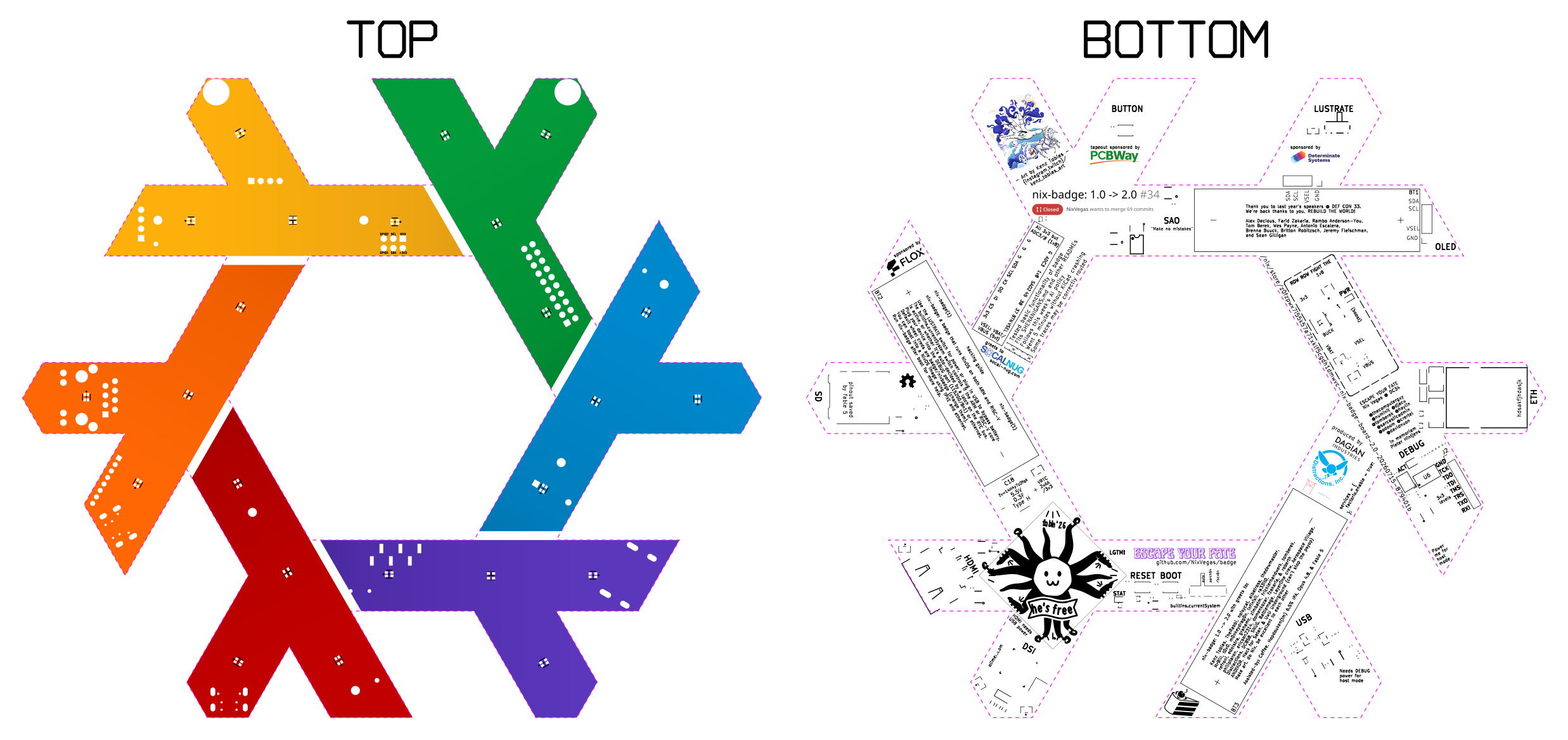
Example reference photo.
PCBWay can print normal silkscreen alongside colored silkscreen, but you may not want to do this. The quality of our PCBs' silkscreen was amazing after we clarified that we did not want normal silkscreen and only wanted color, which was a mistake we made when setting up our PCB order. In fact, I suggest just not using normal silkscreen and using only color, and exporting your board text and footprint markers to be part of the color silkscreen images. Our build process did this for us, and the results were amazingly high quality. The alignment between the silkscreen and solder mask was also flawless, which allowed us to include some of our art as solder mask knockout, but even better than last year.
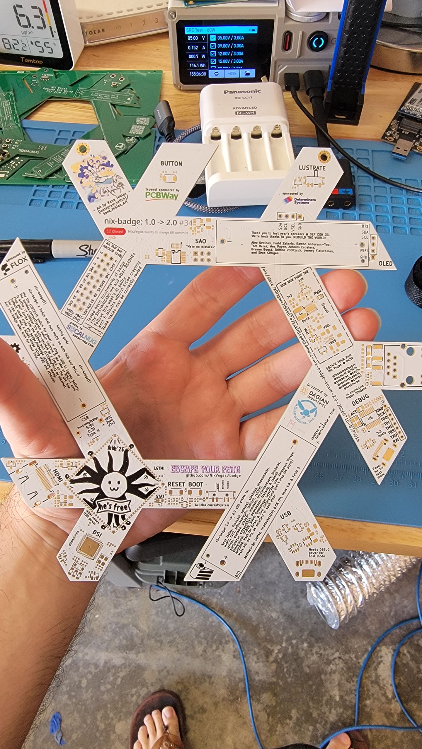
And the full rear view.
PCBWay can print a serial number on your design if they see a part of your normal silkscreen layers that indicates it. We accidentally baked the "WayWayWay" marker into our colored silkscreen, so got asked where the placeholder for our serial number was since it was indicated on our order but we did not have normal silkscreen layers that contained it. We ultimately decided to change the order so it didn't have PCBWay's serial number on the silkscreen, and ended up with an unwanted but ultimately not dealbreaking literal "WayWayWay" on the UV process layer. This basically just can't go on the color silkscreen layer and has to go on the normal one. If you don't have a normal silkscreen layer, you have to get rid of it, but this is not called out explicitly.
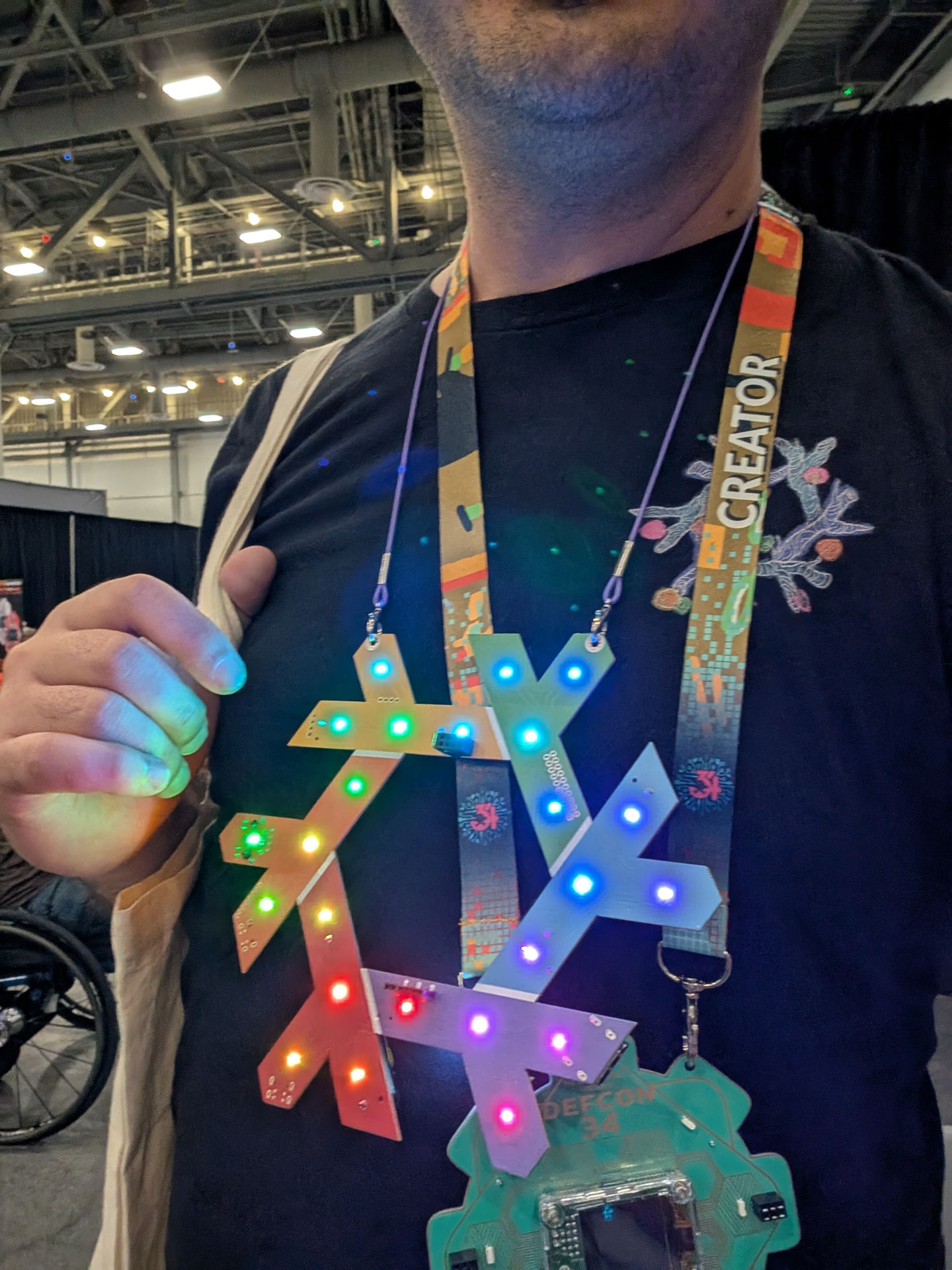
Dan rockin' these colors year round.
Overall, the process had its gotchas but the results speak for themselves. The boards turned out amazingly, and we are incredibly grateful to PCBWay's team for their work fabricating and assembling them for us.
Supply chain
It's a mess.
The normal passives and power circuitry, and even some digital components like gates, buffers, and FETs were fine. Many active components such as our HDMI bridge were either between supply cycles or just difficult to track down.
The Milk-V Duo Module 01 was the largest single problem in the design, and there was a very high chance we just wouldn't get it this year. June and July created a contrast to the situation in February, which is when we scoped it out and it appeared much easier.
We ended up eventually contacting Radxa which gave us a minimum and a quote that would have arrived long after DEF CON. We may still take them up on that if we get enough interest to do a second run.
The interim situation, however, was bad enough, with almost every seller we found on Alibaba claiming they had stock, only for it to mysteriously evaporate when we pressed them on it. Always contact the seller.
After long enough, we made the call for PCBWay to leave the SoM unpopulated. We would do it ourselves. Somehow.
The team that couldn't stop
OK, that's already a lot about the hardware design and procurement process, and we're already on the topic. Let's talk about lead time.
We placed the order in very early July, a full two weeks earlier than last year. That still wasn't enough. The assembled PCBs got here the Friday of DEF CON, and only got to Vegas from San Diego through a heroic effort from one of our team members (thank you Grant).
But they still were missing the Duo Module 01 SoMs. Luckily, we found a vendor for the dev boards which were decidedly less cool than our badge, and somehow were cheaper than all the available SoMs we weren't able to find resellers for. After some practice, we hot plated them to 360°C in my garage over video call with a college roommate (thank you RJ) until all the solder around the SoM's castellated edges melted, and pulled them off. After proving that one of them wasn't simply destroyed by the heat by virtue of it booting, we brought 25 of the recovered SoMs to DEF CON.
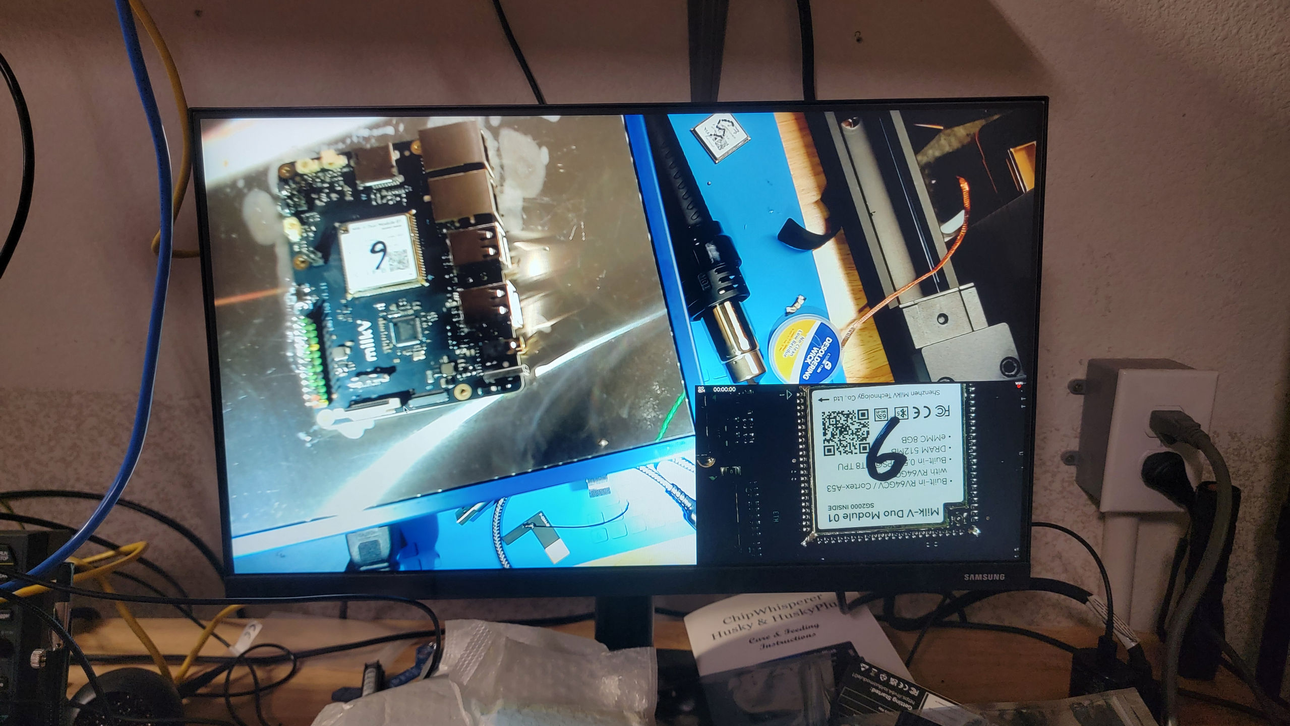
Waiting for reflow over video call
When Grant got to Vegas Friday night, we checked for magic smoke, checked the voltages (3v3 was somewhere between 3.3 and 3.4V, close enough), and experimented with trying to attach the SoM. Ultimately, plenty of flux and solder paste did the job with a high-precision iron. After flashing a very beta firmware and solving what turned out to be a component placement problem that broke ethernet with our soldering irons, we had a single badge working for Saturday.
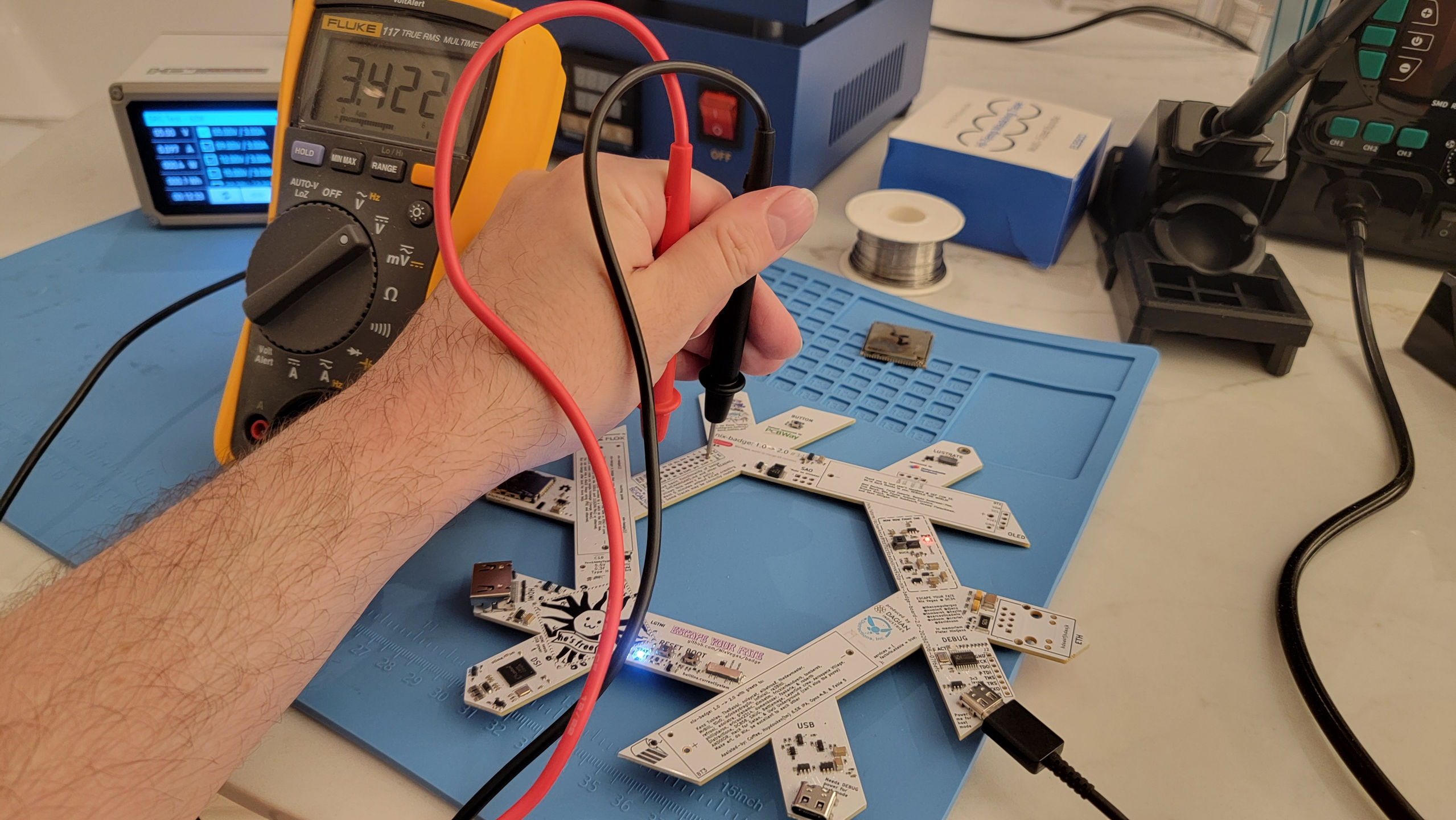
Close enough.
Saturday night was the production run. We had a four stage pipeline. I'd solder the SoM and poweron check it via my portable supply, Tristan would flash and insert an SD card, Dan would add through-hole components and clean the board with ethanol, and it'd be back to Tristan for the final check and bagging. After flashing the final SD cards for our speakers, we got the badges out to them Sunday.
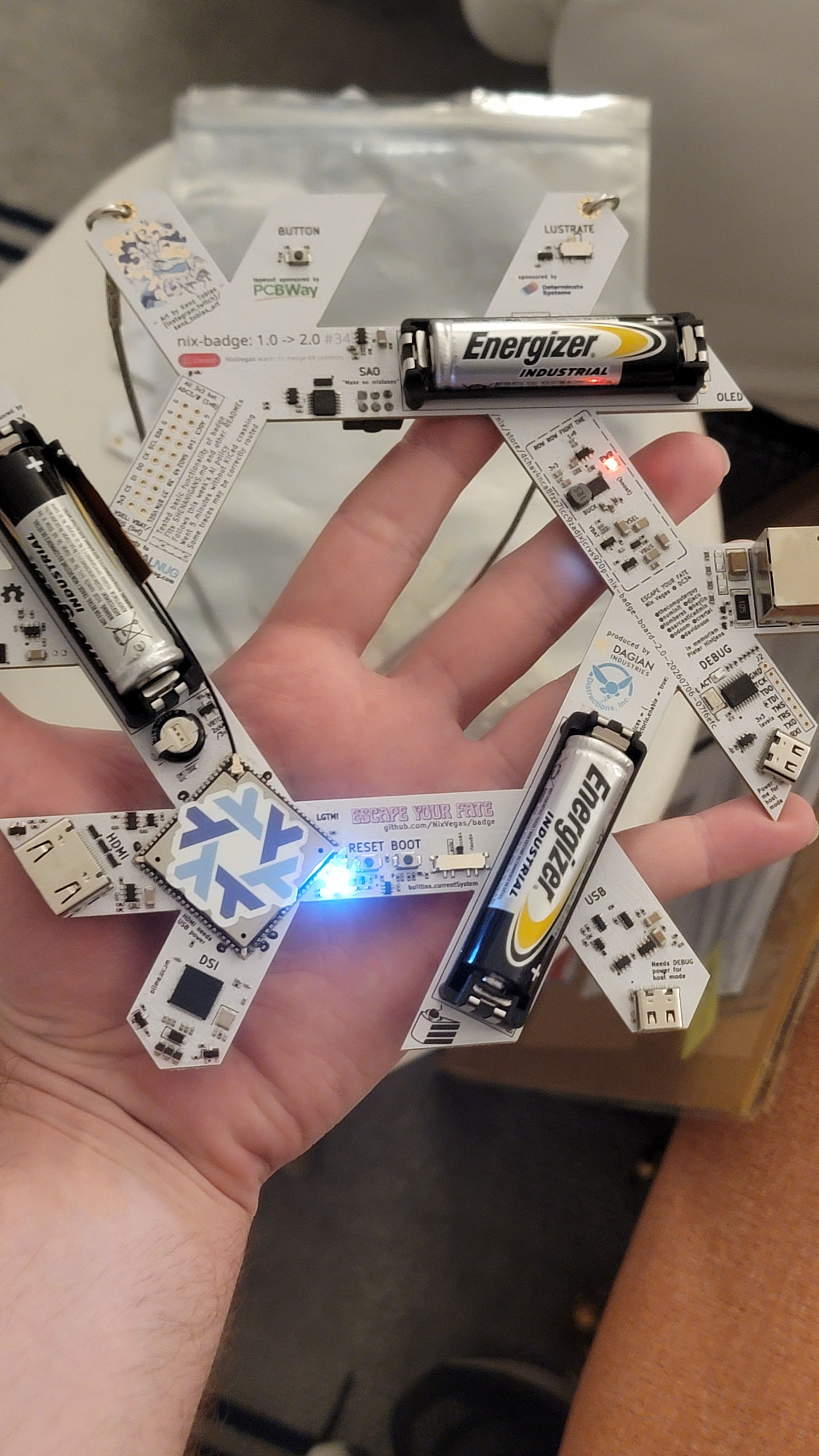
Holding the first-ever NixOS Badge
We didn't do a prototype run because of supply chain lead time, and got 80% yield after we soldered the badges in our room in the Fontainebleau. 5 out of 25 of them were dead, likely just due to SMD soldering mistakes on my part. We'd go on to recover most of these on new boards.
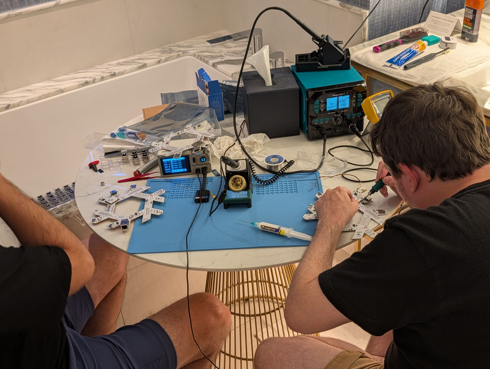
OK, it was late, and we only wore safety glasses most of the time.
... Wait, what?
Yep, that's right, that design review from Fable allowed us to oneshot working PCBs to and from Shenzhen with 80+% yield. They're a .0 release, so there are minor hardware bugs (voltage dividers for battery measurement were too high resistance to always get accurate reads via our ADC), but still. When it booted and we got ethernet working, we cracked open beers at midnight because we did it. We knew that we could hand them out to our speakers with a little more work.
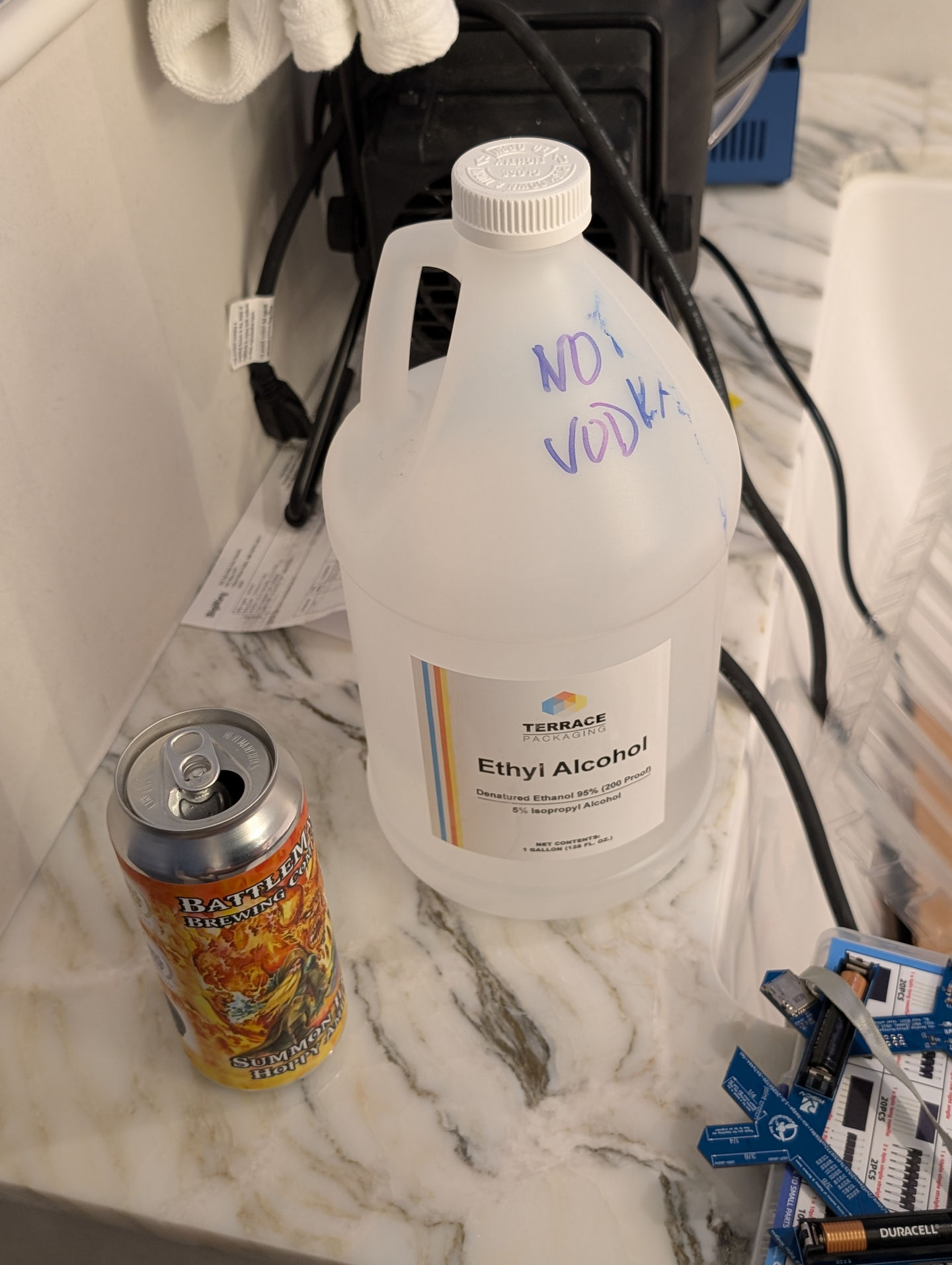
Beer on the left. Ethanol/isopropyl mix on the right. Do not confuse them.
Hacking
The first firmware we shipped was very "version 2.0." It could dual-boot ARM and RISC-V with some sweet LED patterns (and we took them to parties Sunday night), but the software could use some love.
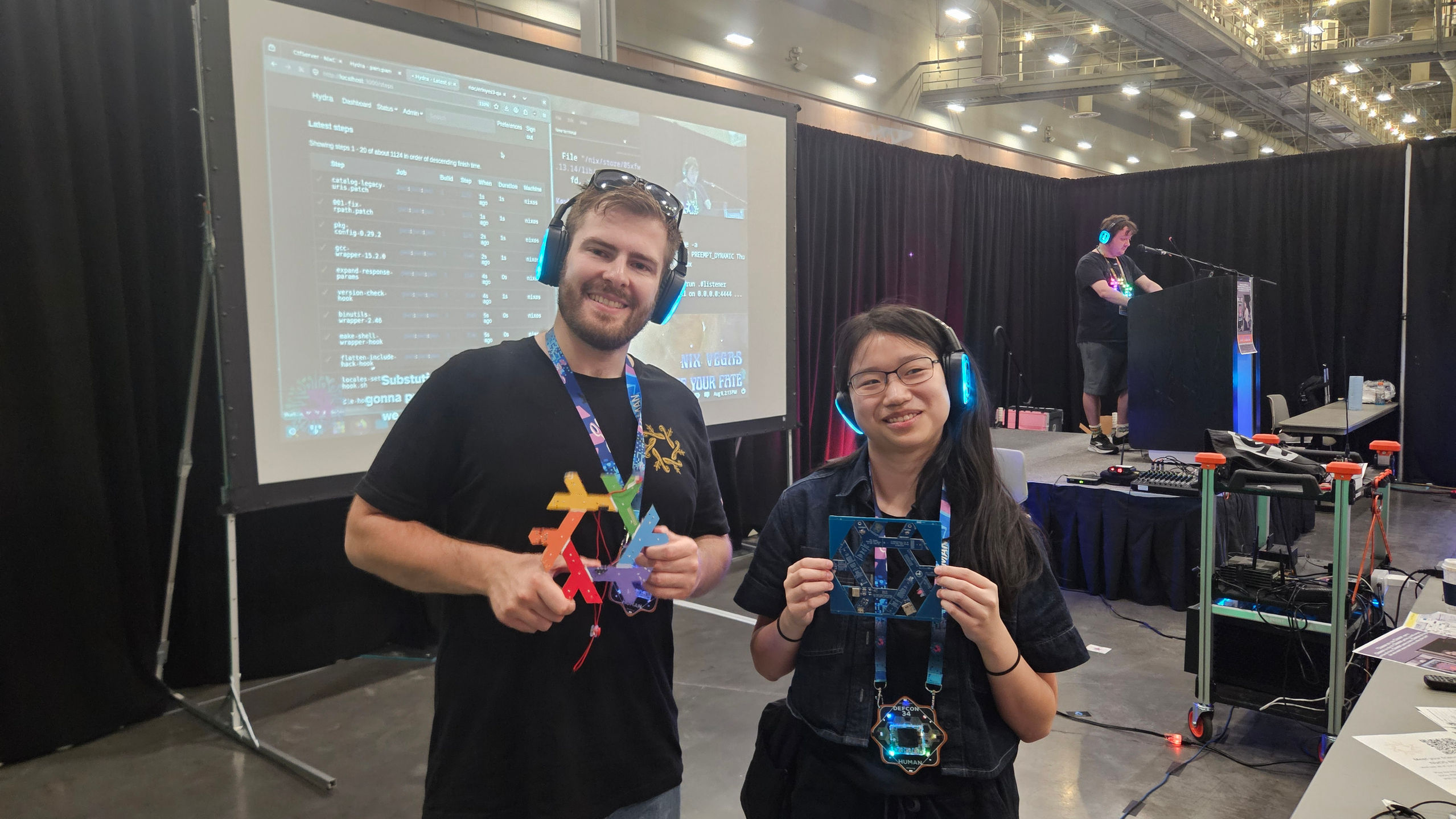
Giving a Nix Badge v2 and v1 to the NixCTF winners (while live pwning hydra in the background)
Over the next weeks, we turned it into something a bit more polished, though that's for a future blogpost.
Conclusion
Thank you again to PCBWay for sponsoring the PCB fabrication, and to the advance readers of this blogpost. We hope to do this again next year!
From the Nix Vegas #badgelife team to you, party on (and maybe see you at Gothcon next year)